

The vast majority of EV traction motors must be supplied with sinusoidal 3-phase alternating current with the frequency proportional to RPM, and the overwhelmingly favorite way to do this is with a triple half-bridge voltage source inverter, or VSI.
In this topology, each bridge switch can connect its output terminal (i.e. motor phase winding) either to the positive or the negative rail of a voltage source (i.e. the battery in an EV, hereafter referred to as +Vbatt and -Vbatt), ignoring the useless choice of both switches being off, and the destructive choice of both being on, hence this type of inverter is further described as “2-level.”
The output waveform of a 2-level inverter operating at the fundamental frequency is a square wave, and while it is possible to drive AC motors with square waves, they don’t much like it because of the high harmonic content, which produces excessive heating, a reduction in maximum achievable torque at any RPM, and more vibration. The traditional approach to reducing the harmonic content is by chopping each output pulse up into many slices and modulating their on times, or duty cycles, sinusoidally. The inductance of the motor windings then integrates this pulsating voltage waveform into a sinusoidal current, with a consequent improvement in torque, vibration and losses. The higher the PWM frequency—i.e. the more slices for each output pulse—the lower the total harmonic distortion, or THD, in the current waveform, which can only be a good thing…up until it isn’t, anyway.
The first major obstacle to increasing the PWM frequency without end is that the percentage of time spent in the switching transitions (i.e. off to on and on to off) increases unless the switches are also proportionally faster. As the switch effectively acts like a resistor during the transitions, these so-called switching losses increase with PWM frequency, all else being equal. However, employing faster switches—such as the latest technology SiC MOSFETs and GaN HEMTs (High Electron Mobility Transistors)—leads to its own set of headaches, as just because you can switch 400 to 800 V in 10-30 ns with these technologies doesn’t mean you should; the extremely high dV / dt of such rapid switching produces prodigious amounts of RF noise, and also causes winding insulation and shaft bearing-destroying common-mode currents to flow. In fact, a rule of thumb says that the effective RF bandwidth, in MHz, of a switching transition, in ns, is 350 / dV / dt; e.g. a 10 ns switching time will generate significant RF energy out to 35 MHz.
One solution to soften the switching transitions without slowing down the switches is to add an LC low-pass filter directly after each inverter output (especially if the motor is more than a few meters away, as the interconnect cables make embarrassingly good radio antennas). Setting the filter’s cutoff frequency to 1/10th the effective bandwidth frequency as calculated above (e.g. 3.5 MHz for the previous example) will suffice for softening the transitions, which will drastically reduce offending RF noise emissions while not introducing enough phase shift to cause problems with vector motor control schemes. These so-called dV / dt filters won’t help much with reducing the common-mode currents, though, as the motor voltage waveform will still very much consist of pulses that span the full battery voltage.
To effectively integrate the chopped voltage waveform into a nice sine wave (i.e. same as the current waveform) would require the LC filter cutoff frequency be no higher than 1/10th the actual PWM frequency, and that would take up a lot more volume (and cost more) while almost certainly introducing enough phase shift to interfere with vector control schemes if not addressed in hardware and/or software.
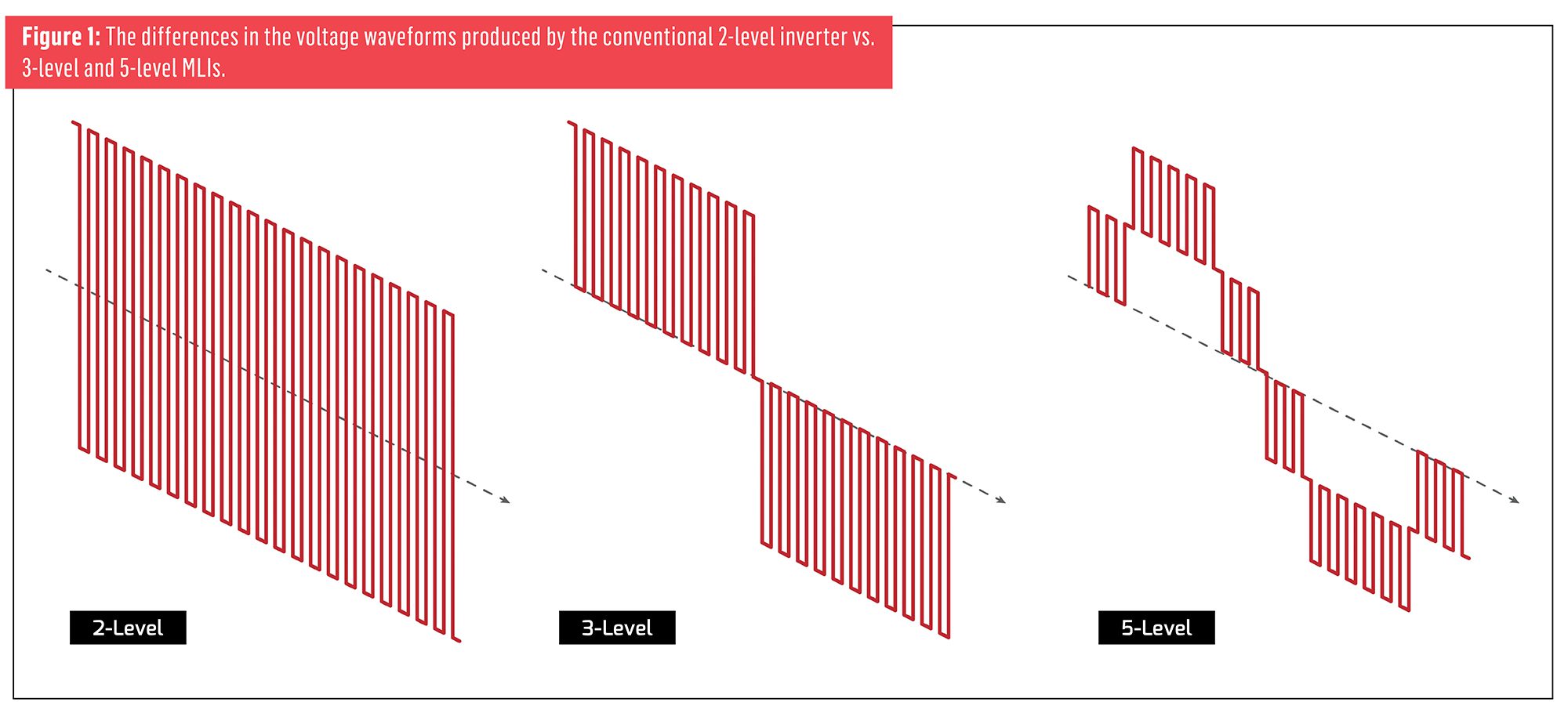
Another way to lower the THD and reduce the magnitude of common-mode currents is to add more steps to the voltage waveform generated by the inverter—a multilevel inverter, or MLI, in other words. Figure 1 illustrates the differences in the voltage waveforms produced by the conventional 2-level inverter vs 3-level and 5-level MLIs. It’s difficult to see how the 2-level inverter even produces a sinusoidal current, whereas it’s much more obvious in the 3-level and 5-level MLIs. Note also that each PWM pulse in the 2-level inverter swings the full battery voltage, but only half Vbatt for the 3-level MLI, and a quarter of Vbatt for the 5-level MLI, etc. The price you pay for lower THD and common mode currents at a given PWM frequency with all multilevel inverter topologies is that they are much more complicated than their 2-level progenitor (ridiculously so, in some cases), and might very well not be worth paying for when compared to the more band-aid-type solutions of additional LC filtering, hardening of the motor against common-mode currents, etc.
Multilevel inverters obviously need access to separate voltage sources for each output voltage level, or else must create the voltage levels indirectly.
Multilevel inverters obviously need access to separate voltage sources for each output voltage level (and each motor phase, for some MLI topologies), or else must create the voltage levels indirectly (typically with capacitive voltage dividers). An example of the former type of MLI is the Cascaded H-Bridge, which has found some use in industrial applications because the separate DC voltages can be supplied by a mains transformer with multiple secondaries, but won’t be considered further here because it would require a Rube Goldberg-like arrangement of isolated battery packs and chargers in an EV.

A far simpler way to generate the different voltage levels is the capacitive voltage divider (examples of such for 3- and 5-level MLIs shown in Figure 2), which acts just like a resistive voltage divider, though only for alternating currents. Wiring two equal-value capacitors in series will divide the bus voltage in half, and the midpoint will become a new 0 V reference for the MLI (i.e. the power stage of a 3-level MLI generates pulses with amplitudes of +Vbatt / 2, 0 V, or -Vbatt / 2, with respect to the midpoint).
The divider function can be extended by adding more pairs of capacitors, in which case the midpoint of each junction becomes a new voltage level (so the 4-capacitor divider string for a 5-level MLI creates voltage levels of +Vbatt / 2, +Vbatt / 4, 0 V, -Vbatt / 4 and -Vbatt / 2, once again assuming all capacitor values are equal).
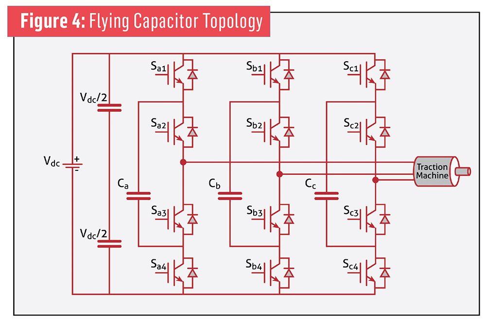
Neutral Point Clamped and Flying Capacitor types of multilevel inverter topologies use the same basic power stage structure but different methods of generating the 0 V output level.
As advantageous as reducing the voltage swing of the pulses might be, the law of diminishing returns will kick in at some point, as the sheer volume of the capacitors required—and the complexity of the rest of the MLI—scales directly with the number of voltage levels. It is also important to note that the capacitors in the voltage dividers have to carry considerable ripple current, both at the fundamental (motor) frequency and the PWM frequency, meaning that they will likely need to have relatively large capacitance values (to minimize ripple voltage from the low-frequency currents) and a film dielectric (to minimize losses from the high-frequency currents), which is not terribly cost- or volume-effective.

Two of the original multilevel inverter topologies that could be used in EVs are the Neutral Point Clamped (NPC) and Flying Capacitor (FC) types, shown in Figures 3 and 4, respectively, which use the same basic power stage structure but different methods of generating the 0 V output level. In each of these 3-level MLIs, a phase winding is connected to +Vbatt when the upper two switches are on, or -Vbatt when the lower two switches are on, but the 0 V output level is generated directly in the NPC type by turning on the inner two switches, while in the FC type it is generated indirectly by turning on the upper and lower-inner switches at the same time to charge the flying capacitor, followed by the upper-inner and lower switches to discharge it. Neither of these methods allow for actively balancing charge on the divider capacitors, so there tends to be more voltage ripple across them, and as mentioned above, the more ripple on the divider capacitors, the higher the THD. The NPC type is easier to control (far easier, in fact), while the FC type has higher fault tolerance (a capacitor is in series with the motor windings during the 0 V state) and can achieve a lower ultimate THD, but it is fiendishly difficult to control and introduces the thorny problem of how to pre-charge its flying capacitors during startup.
Two MLI topologies that use active switches to better maintain charge balance on their divider capacitors while preserving the ability to handle loads with a wide power factor range (read: induction motors) are the Active Neutral Point Clamped (ANPC) and the T-type, shown in Figures 5 and 6, respectively.
The ANPC MLI replaces the clamping diodes in the NPC with switches that are turned on in conjunction with their respective middle bridge switch to clamp that winding to a capacitor midpoint. The key difference in operation compared to the passive clamping with diodes is that the on time of the clamping switches can be varied to better control the charge balance on the divider capacitors.

The T-type MLI operates in a similar fashion but saves two switches by replacing the clamping and inner bridge switches with a single bidirectional switch (composed of two conventional unidirectionally-blocking switches wired back-to-back) that directly connects a phase winding to a divider midpoint while allowing for bidirectional current flow when on, and bidirectional blocking when off. The main advantage of the T-type inverter is that it uses a standard triple half-bridge for driving the motor, but that also means the bridge switches must be rated to comfortably withstand the full battery voltage, whereas all of the other MLI topologies considered here stack two switches in series at the outer (highest voltage) bridge positions (the inner switches only see a fraction of Vbatt), so all of the switches can theoretically be rated for half the blocking voltage (in a 3-level MLI). That’s particularly helpful for current-technology GaN HEMTs as they most commonly top out at a 650 VDC rating, but not so relevant with SiC MOSFETs (or older-technology Si IGBTs) as they are widely available in the 1.2 kV and 1.7 kV ratings that would be appropriate for battery voltages in the 600-800 VDC range.

There are numerous other MLI topologies that are even more complex, but they won’t be considered here—the considerable increase in component count going from a 2-level VSI to any of the 3-level (much less 5-level!) MLI topologies is enough of an obstacle to their adoption as it is. Another obstacle is that all of the MLI topologies require changes to the power stage switch control schemes, which means their development will be far more costly (and take more time than anticipated—but isn’t that always the case?). When one also considers that just the AC voltage divider capacitors required by most MLI topologies will likely take up as much volume all by themselves as a complete 2-level VSI (to say nothing of the flying capacitors also required in the FC MLI), and that a substantial reduction in RF noise emissions—and even common-mode noise currents—can be achieved in the 2-level VSI simply by adding LC filters to each phase output, the argument for MLIs in EVs is a tough one to sell.
This article first appeared in Issue 70: October-December 2024 – Subscribe now.

